
产品分类
MAX2062
The MAX2062 high linearity, dual analog/digital variable/gain amplifier (VGA) operates in the frequency range of 50MHz to 1000MHz, with two independent attenuators for each signal path.
Due to each stage having its own external RF input and RF output, this component can be configured to optimize noise figure (NF) (first configure amplifier), OIP3 (last configure amplifier), or a compromise between NF and OIP3.
In addition, the device can operate on a single+5V power supply, with full performance or+3.3V power supply to achieve a lower performance enhanced energy-saving mode.
MAX2062 General Description:
The MAX2062 high-linearity, dual analog/digital variable/gain amplifier (VGA) operates in the 50MHz to 1000MHz frequency range with two independent attenuators in
each signal path. Each digital attenuator is controlled as a slave peripheral using either the SPI-compatible interface, or a 5-bit parallel bus with 31dB total adjust-ment range in 1dB steps. An added feature allows rapid-fire gain selection among each of the four steps, preprogrammed by the user through the SPI-compatible interface. A separate 2-pin control lets the user quickly access any one of four customized attenuation states without reprogramming the SPI bus. Each analog attenu-ator is controlled using an external voltage or through the SPI-compatible interface using an on-chip 8-bit DAC.
Since each of the stages has its own external RF input and RF output, this component can be configured to either optimize noise figure (NF) (amplifier configured first), OIP3 (amplifier last), or a compromise of NF and OIP3. The device’s performance features include 24dB amplifier gain (amplifier only), 7.3dB NF at maximum gain (includes attenuator insertion losses), and a high OIP3 level of +41dBm. Each of these features makes the device an ideal VGA for multipath receiver and trans-mitter applications.
In addition, the device operates from a single +5V supply with full performance or a +3.3V supply for an enhanced power-savings mode with lower performance. The device is available in a compact 48-pin TQFN package (7mm x 7mm) with an exposed pad. Electrical performance is guaranteed over the extended tempera-ture range, from TC =-40NC to +85NC.
MAX2062 Features:
Independently Controlled Dual Paths
50MHz to 1000MHz RF Frequency Range
Pin-Compatible Family Includes
MAX2063 (Digital-Only VGA)
MAX2064 (Analog-Only VGA)
19.4dB (typ) Maximum Gain
0.34dB Gain Flatness Over 100MHz Bandwidth
64dB Gain Range (33dB Analog Plus 31dB Digital)
56dB Path Isolation (at 200MHz)
Built-In 8-Bit DACs for Analog Attenuation Control
Supports Four Rapid-Fire Preprogrammed
Attenuator States
Quickly Access Any One of Four Customized
Attenuator States
Ideal for Fast-Attack, High-Level Blocker
Protection
Protects ADC Overdrive Condition
Excellent Linearity (Configured with Amp Last at 200MHz)
+41dBm OIP3
+56dBm OIP2
+19dBm Output 1dB Compression Point
7.3dB Typical Noise Figure (at 200MHz)
Fast, 25ns Digital Switching
Very Low Digital VGA Amplitude Overshoot/Undershoot
Single +5V Supply (or+3.3V Operation)
Amplifier Power-Down Mode for TDD Applications
MAX2062 Applications:
IF and RF Gain Stages
Temperature-Compensation Circuits
GSM/EDGE Base Stations
WCDMA, TD-SCDMA, and cdma2000M Base
Stations
WiMAXM, LTE, and TD-LTE Base Stations and
Customer-Premise Equipment
Fixed Broadband Wireless Access
Wireless Local Loop
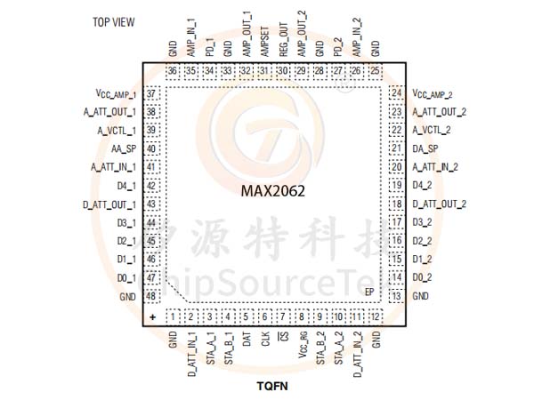
MAX2062 Pin Configuration:
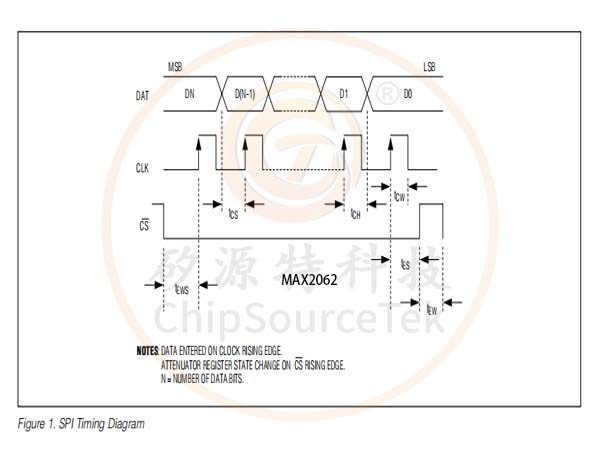
 MAX2062 SPI Timing Diagram:
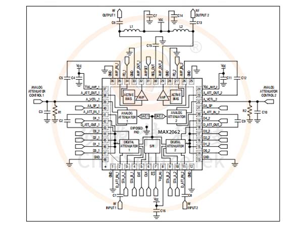
 MAX2062 Typical Application Circuit:

The MAX2062 high-linearity, dual analog/digital variable/gain amplifier (VGA) operates in the 50MHz to 1000MHz frequency range with two independent attenuators in
each signal path. Each digital attenuator is controlled as a slave peripheral using either the SPI-compatible interface, or a 5-bit parallel bus with 31dB total adjust-ment range in 1dB steps. An added feature allows rapid-fire gain selection among each of the four steps, preprogrammed by the user through the SPI-compatible interface. A separate 2-pin control lets the user quickly access any one of four customized attenuation states without reprogramming the SPI bus. Each analog attenu-ator is controlled using an external voltage or through the SPI-compatible interface using an on-chip 8-bit DAC.
Since each of the stages has its own external RF input and RF output, this component can be configured to either optimize noise figure (NF) (amplifier configured first), OIP3 (amplifier last), or a compromise of NF and OIP3. The device’s performance features include 24dB amplifier gain (amplifier only), 7.3dB NF at maximum gain (includes attenuator insertion losses), and a high OIP3 level of +41dBm. Each of these features makes the device an ideal VGA for multipath receiver and trans-mitter applications.
In addition, the device operates from a single +5V supply with full performance or a +3.3V supply for an enhanced power-savings mode with lower performance. The device is available in a compact 48-pin TQFN package (7mm x 7mm) with an exposed pad. Electrical performance is guaranteed over the extended tempera-ture range, from TC =-40NC to +85NC.
MAX2062 Features:
Independently Controlled Dual Paths
50MHz to 1000MHz RF Frequency Range
Pin-Compatible Family Includes
MAX2063 (Digital-Only VGA)
MAX2064 (Analog-Only VGA)
19.4dB (typ) Maximum Gain
0.34dB Gain Flatness Over 100MHz Bandwidth
64dB Gain Range (33dB Analog Plus 31dB Digital)
56dB Path Isolation (at 200MHz)
Built-In 8-Bit DACs for Analog Attenuation Control
Supports Four Rapid-Fire Preprogrammed
Attenuator States
Quickly Access Any One of Four Customized
Attenuator States
Ideal for Fast-Attack, High-Level Blocker
Protection
Protects ADC Overdrive Condition
Excellent Linearity (Configured with Amp Last at 200MHz)
+41dBm OIP3
+56dBm OIP2
+19dBm Output 1dB Compression Point
7.3dB Typical Noise Figure (at 200MHz)
Fast, 25ns Digital Switching
Very Low Digital VGA Amplitude Overshoot/Undershoot
Single +5V Supply (or+3.3V Operation)
Amplifier Power-Down Mode for TDD Applications
MAX2062 Applications:
IF and RF Gain Stages
Temperature-Compensation Circuits
GSM/EDGE Base Stations
WCDMA, TD-SCDMA, and cdma2000M Base
Stations
WiMAXM, LTE, and TD-LTE Base Stations and
Customer-Premise Equipment
Fixed Broadband Wireless Access
Wireless Local Loop
MAX2062 Pin Configuration:

请提交您的基本信息,发邮件Sales@ChipSourceTek.com,或者打电话给我们,13823761625(微信同号),我们将会尽快与您联系!

关注矽源特公众号

矽源特微信客服
 发送邮件
发送邮件 商务QQ客服
 13823761625
