


TRSP(M)5040A General Descriptions/一般说明:
TRSP(M)5040A系列是4位微控制器,可播放4通道旋律或4通道ADPCM与PWM直接驱动电路。PWM的分辨率为8/10/12位。它们包括一个低成本、高性能的CMOS微处理器。该上升的时钟频率通常为8.192(±3%)MHz。该芯片可在2.0V~5.5V的较宽电压范围内工作。它在内部包含程序ROM(PROM)和数据ROM(DROM)。
程序ROM的最大大小为4K字,最大数据ROM大小为120K字节。最大工作SRAM为(128+2)缺口。它共提供了12个软件可编程的I/O端口。
TRSP(M)5040A series are 4-bits micro-controller which could play 4 channel melody or 4 channel ADPCM with PWM direct drive circuit. PWM resolution is 8/10/12 bits. They includes a low cost, high performance CMOS micro-processor. The clock frequency of this up is typically 8.192 (±3%) MHz. This chip operates over a wide voltage range of 2.0V~5.5V. It contains program ROM (PROM) and data ROM (DROM) inside.
The maximum program ROM is 4K words and maximum data ROM size is 120K byte. The maximum working SRAM is (128+2) nibbles. It is provided with total 12 software programmable I/O Ports.
TRSP(M)5040A Features/特性:
Operating voltage: 2.0V to 5.5V
MCU Operation frequency: 8.192MHz
Memory Size
Program ROM size: 4K*12-bits OTP type
Data ROM size: Maximum 120K*8-bits OTP type
SRAM size: 128*4 bits
User register: 2*4 bits
Wakeup function for power-down mode:
HALT mode wakeup source: Port A, Port B and Port E/CE can wake-up from HALT mode to NORMAL mode and executing wake-up sub-routine program.
8 input/output pins: Port A and Port B can be defined as input or output port bit by bit.
4 input/output ports or 4 input only ports or 4 output only ports “Port CE/E/C” defined by option:
If input only ports are employed, Port E defined as input only ports.
If output only ports are employed, Port C defined as output only ports.
If input/output ports are selected, Port CE defined as input/output ports bit by bit.
Four reset condition:
Low voltage reset. (LVR = 2.0V)
Power on reset.
External reset pin. (active low)
Watch dog timer overflow.
One internal interrupt sources:
PWM interrupt.
WDT
Watch dog timer, can enabled/disabled by option.
WDT period is 256*256*16/Fsys. (WDT period is 0.13 sec for system clock=8.192MHz)
Audio output:
Support PWM or DAC mode by option.
Support 8/10/12 bits.
Support option set for pull down resistor 1M, 50K or 220K Ohm, reset pin (PB3 or PC3), low voltage reset…etc.
Oscillator fuse option ±3%, temperature & voltage compensation.
Support security option (1 bit) for read inhibition.
Support 16-levels LVD function.
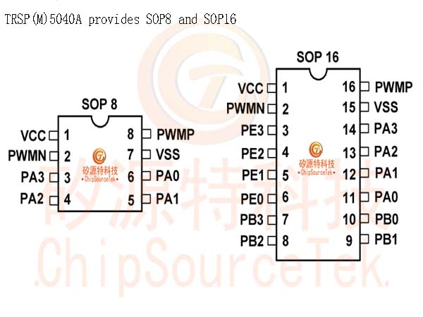
TRSP(M)5040A Package:
5040A YJT.jpg)
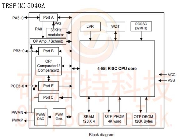
TRSP(M)5040A Block Diagram:
5040A KT.jpg)
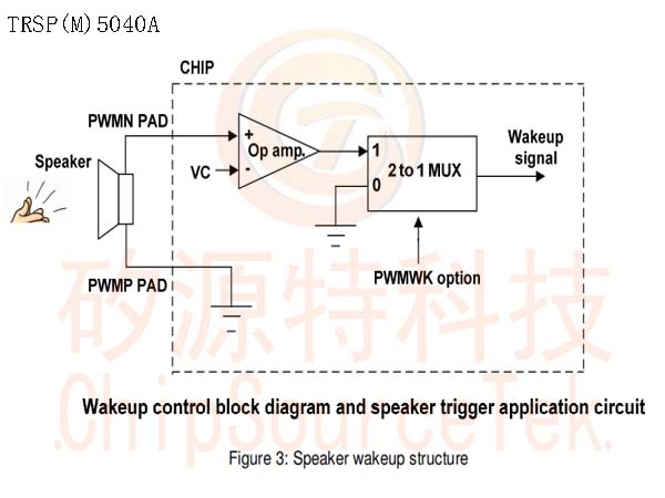
TRSP(M)5040A Speaker wakeup structure:
5040A T1.jpg)
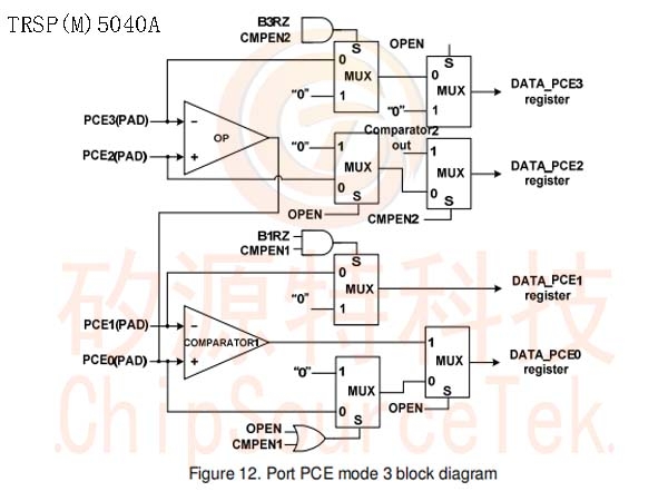
TRSP(M)5040A Port PCE mode 3 block diagram:
5040A PCE.jpg)
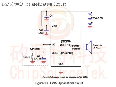
TRSP(M)5040A The Application Circuit:
5040A YYT.jpg)
5040A YYT2.jpg)


 Business consulting

 13823761625
 Mail me