


LX1022概述:
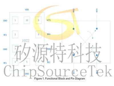
The LX1022 is a CMOS, Silicon-On-Insulator (SOI) double-pole, double-throw (DPDT) switch. The switch provides high linearity performance, low insertion loss and high isolation.
Switching is controlled by one control voltage pin, VCTL. Depending on the logic voltage level applied to this pin, the RF1 and RF2 pins connect to one of the two other RF3 and RF4 pins through a low insertion loss path, while maintaining a high isolation path to the alternate port, ANT. No external DC blocking capacitors are required on the RF path as long as no DC voltage is applied externally.
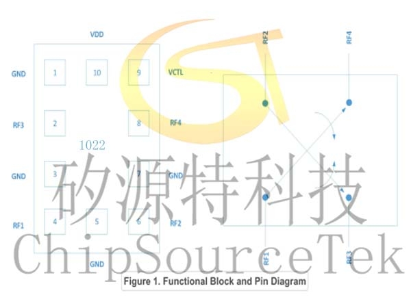
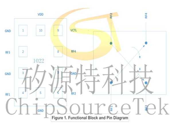
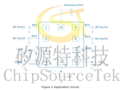
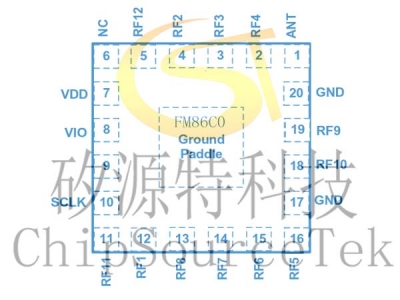
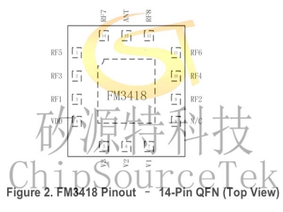
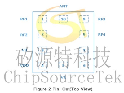
The LX1022 DPDT switch is provided in a QFN 10- pin, 1.1mm x 1.5mm x 0.45mm package. The functional block diagram and the pin configuration are shown in Figure 1. Signal pin assignments and functional pin descriptions are provided in Table 1.
LX1022特性:
Broadband frequency range: 619 to 5925MHz
GPIO interface
RoHS compliant package
Compact 1.1mm x 1.5mm x 0.45mm QFN 10-pin package, MSL1
LX1022应用:
2G/3G/4G/5G antenna swapping
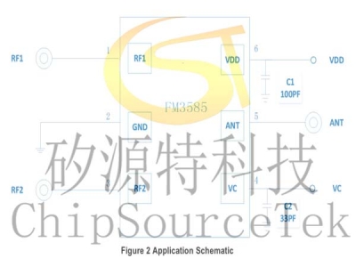
LX1022功能方块及引脚图:
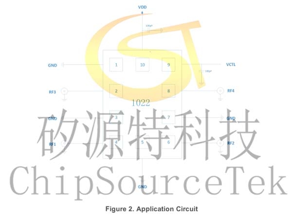
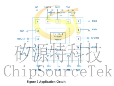
LX1022应用电路:

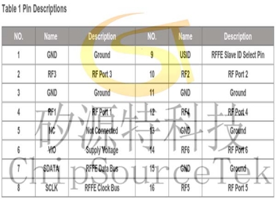
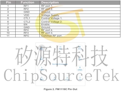
LX1022引脚描述:
|
No.
|
Name
|
Description
|
No.
|
Name
|
Description
|
|
1
|
GND
|
Ground
|
6
|
RF2
|
RF Port2
|
|
2
|
RF3
|
RF Port3
|
7
|
GND
|
Ground
|
|
3
|
GND
|
Ground
|
8
|
RF4
|
RF Port4
|
|
4
|
RF1
|
RF Port1
|
9
|
VCTL
|
Control Voltage Pin
|
|
5
|
GND
|
Ground
|
10
|
VDD
|
DC Power Supply
|
Table 2. VCTL Truth Table for RF Channel Operating Modes
| VCTL | RF Channel Operating Modes |
| Low | RF1 to RF3 On, RF2 to RF4 On |
| High | RF1 to RF4 On, RF2 to RF3 On |
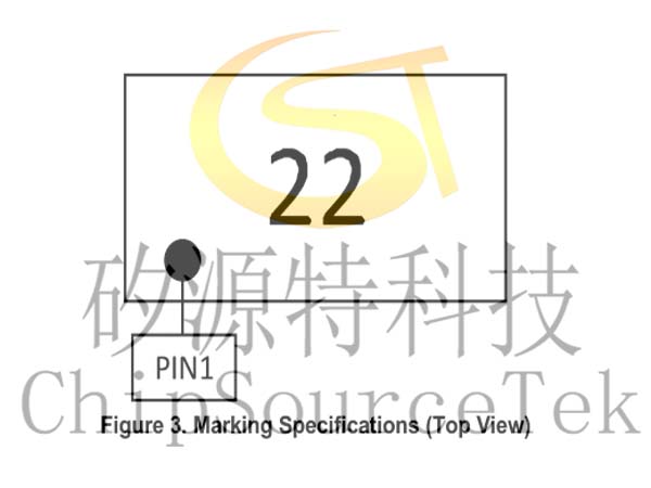
LX1022Marking Specifications:


 Business consulting

 13823761625
 Mail me